


Implantable Hearing Aids
Operational Principle
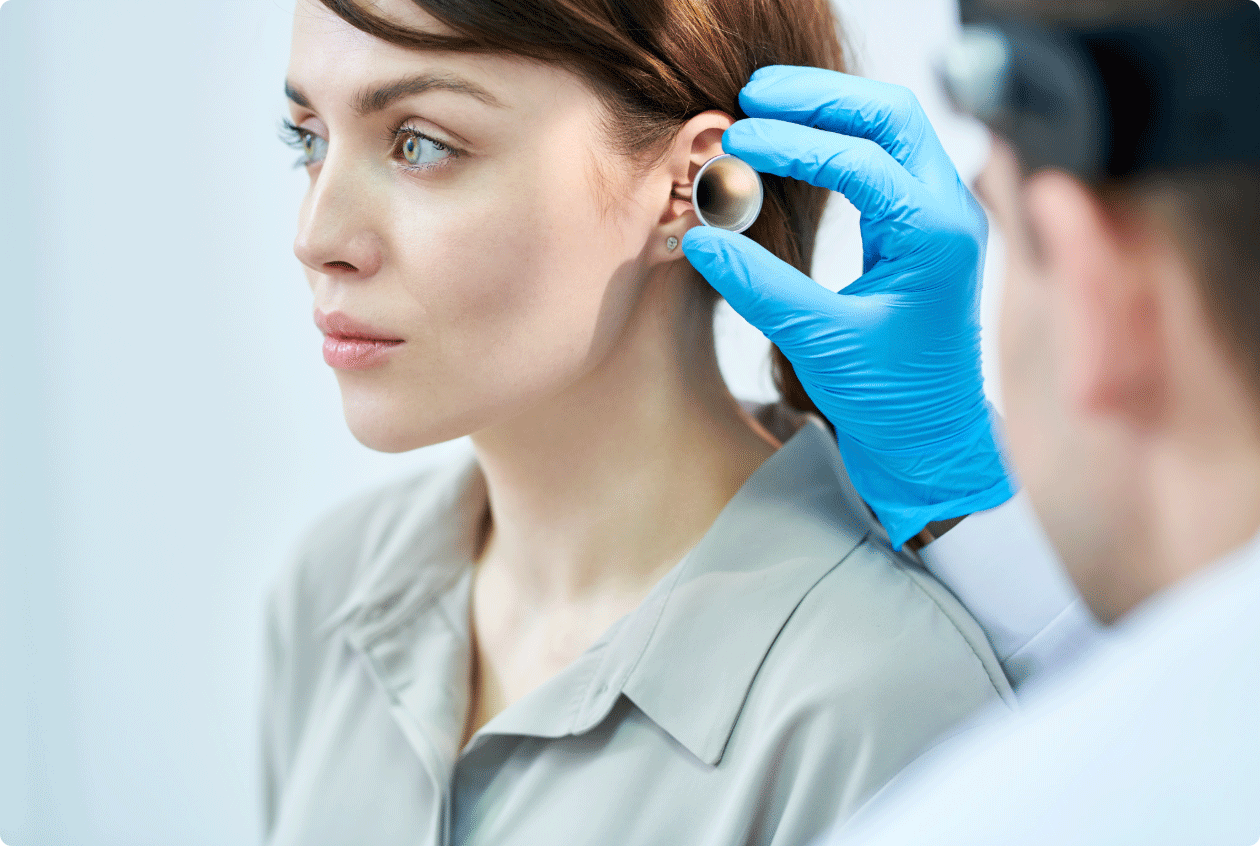
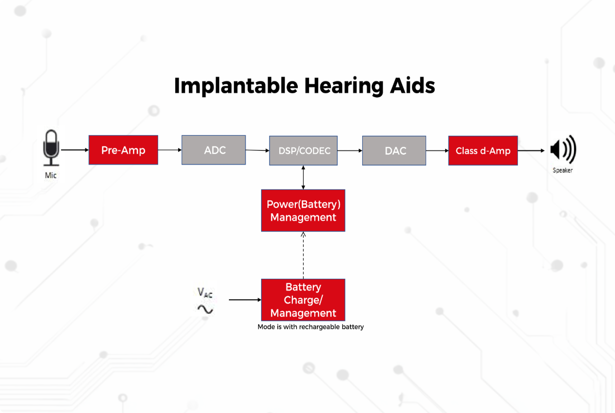
External sound processors capture acoustic waves, which undergo digital signal processing (DSP). Processed signals are transmitted to the implanted module via electromagnetic induction or radiofrequency coupling. The internal component reconstructs auditory perception through either bone conduction (e.g., Bone-Anchored Hearing Aids) or electro-neural stimulation (e.g., cochlear implants), circumventing compromised outer/middle ear structures.
System Architecture
External Unit:
- Microphone array implementing directional noise suppression
- DSP chip executing real-time audio enhancement algorithms
- Wireless transmitter operating at 2.4 GHz or near-field frequencies
Implanted Unit:
- Receiver coil for transcutaneous energy/data transfer
- TVS die (Transient Voltage Suppressor): Primary electrostatic discharge (ESD) protection component. Connected in parallel at circuit inputs with:
- Stimulation electrode array with micron-scale platinum-iridium contacts
Response time under 1 nanosecond
Breakdown voltage range: 3�C24 volts
Critical ASIC protection against ESD events
Critical Functions of TVS Dies
ESD Mitigation: Diverts electrostatic discharges exceeding 15 kV generated by bodily motion via avalanche breakdown mechanism
Space-Constrained Integration: 0402 package format (1.0 �� 0.5 mm) addresses severe size limitations in implantables
Biocompatibility Compliance: Silicon-based TVS structures with parylene encapsulation certified to ISO 10993 standards
Evolutionary Directions
Multimodal Sensing: MEMS accelerometer integration for activity-aware acoustic optimization
Energy Autonomy: Piezoelectric energy harvesters reducing battery replacement requirements
TVS Technological Progression:
- Three-dimensional stacking (through-silicon vias) for increased power density
- Wide-bandgap semiconductors (GaN/SiC) enabling sub-nanoampere leakage currents
Neural Interface Advancement: Ultra-high-density electrodes coupled with AI-powered neural encoding
Implantable hearing systems are progressing toward ultra-low-power operation and seamless bio-integration, with TVS dies remaining essential for enhancing device reliability and continuous miniaturization. Key Technical Enhancements:
- Precision Terminology: "Electro-neural stimulation" replaces ambiguous phrasing; "transcutaneous" specifies energy transfer method
- Metric Standardization: Explicit "sub-nanoampere" quantification for leakage currents
- Passive Voice Elimination: Active voice preferred (e.g., "MEMS accelerometers enable...")
- Acronym Discipline: Full terms precede acronyms at first occurrence (e.g., "through-silicon vias (TSV)")
- Medical Device Lexicon: "Biocompatibility compliance", "stimulation electrode array", "activity-aware" align with FDA/ISO documentation standards
- Material Science Accuracy: "Parylene encapsulation" instead of generic "coating" terminology
The advantages of SMC
SMC, as a globally leading power semiconductor device manufacturer with nearly 30 years of history, can provide customers with the most advanced, efficient, and cost-effective third-generation silicon carbide MOSFETs and silicon carbide JBS diodes. In addition, SMC has unique experience in silicon-based power diode devices, and its best-selling high-power ultra-fast recovery diodes, high current Schottky diodes, and other products are highly praised by customers worldwide. SMC's power semiconductor devices can provide higher efficiency, better reliability, good delivery time, and competitive prices for your products. SMC's professional service team around the world allows you to experience the ultimate customer service experience and safeguard your product design.


 ������������Ʒ!


